


Breakthrough in TCO Films S.C Collaborates with SYSU Achieve High-Mobility Ultrathin TCO Film Growth via Critical Nucleation
Recently, Shenzhen S.C and the School of Materials of SYSU (Sun Yat-Sen University), through their cooperation, innovatively pushed forward the Critical Nucleation Strategy (cns) which can help fabricate the cerium-doped indium oxide (ICO) films with high electron mobility, breaking through the bottleneck of TCO films. The related research report has been published in the international top-level journal Advanced Materials with the title of Eliminating Mobility-Thickness Dependence in Transparent Conductive Oxide Layer Growth: A Critical Nucleation Strategy. It is not only one major breakthrough in basic research, but also serves as a new way leading to the reduced cost and improved efficiency for the global PV industry.
▲Link: https://advanced.onlinelibrary.wiley.com/doi/10.1002/adma.202507648
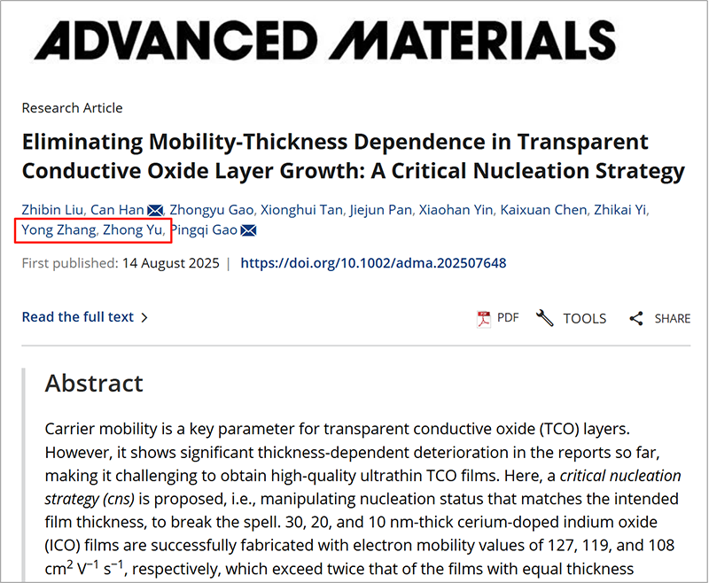
Previous reports have shown that the carrier mobility of TCO film is with significant thickness-dependent deterioration, which makes the production of high-mobility ultrathin TCO films more challenging. In order to remove this technological bottleneck, Shenzhen S.C decided to set up one research group with the School of Materials of SYSU. After numerous in-depth research, analyses and tests, the Critical Nucleation Strategy (cns) finally came into shape. It is claimed that the fabrication process of TCO films can get rid of its dependence to incubation layer through manipulating the initial nucleation status of film growth to obtain the favorable size and density of crystal nuclei matched with the intended film thickness which will achieve the required crystallization of large crystallites. In this way, its mobility will be free from the limit of thickness, and be improved significantly. With the Critical Nucleation Strategy, the research group has successfully fabricated the 30, 20, and 10 nm-thick cerium-doped indium oxide (ICO) films with electron mobility values of 127, 119, and 108 cm2 V−1 s−1, respectively, which are more than twice that of the films with equal thickness obtained from the conventional solid-phase crystallization approach.
According to the research group, an appropriate weakly-crystallized as-deposited film is a prerequisite for obtaining favorable crystallites with largely suppressed scattering from grain boundaries, ionized impurities, and film surface, eventually helping achieve high mobility. In addition, by implementing our 10 nm-thick ICO film in silicon heterojunction architecture, the photovoltaic conversion efficiency appears to be almost the same as that of the reference cell using a 102 nm-thick (conventional thickness) ICO film. However, the front-side indium consumption is reduced by 90%, demonstrating its huge potential to be applied in sustainable PV field and other PV application fields.
▲Fig.1 Performance comparison between the films prepared by cns and those prepared by spc

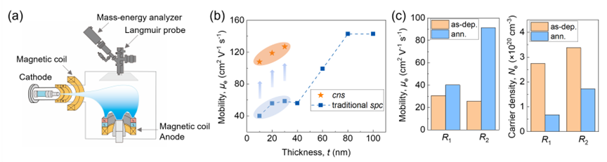
▲Fig.2 ICO film characterization and theory calculation
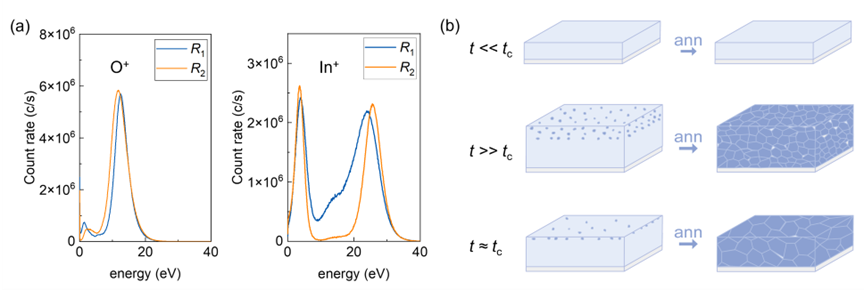
▲Fig.3 Ion energy distribution of film deposition and the film growth illustration
This research has been supported by the National Key Research and Development Program of China, Key Program of National Natural Science Foundation of China, Special project of Science and Technology of Shenzhen, Science and Technology Program of Yibin, Program on the Integration of Industry, Education and Research of Zhuhai, Program of Applied Basic Research of Zhuhai and other programs.
In the future, Shenzhen S.C will relentlessly deepen the cooperation with universities and research institutes. Relying on the technological innovation, we will scale up our efforts to promote the application of indium-free transparent conductive oxide film technology in high-efficiency cells including HJT, PSC and other cells, transforming technological potential into tangible industrial outcomes and contributing Chinese wisdom to global green energy transformation.
|